INTRODUCTION
Taking a closer look at the 1571 disk drive reveals that it contains the major ICs needed to build a 1581 compatible disk drive. This blog describes how to boost a 1571 so that it can turn into a 1581 with the flip of a switch.

FEATURES
- High compatibility 1581 disk drive emulation
- Use of original 1581 DOS
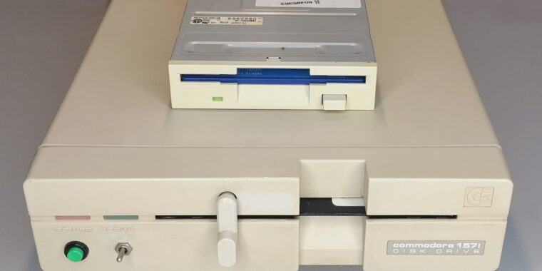
- Standard PC 3.5″ FDD
- No need for extra FDC WD1770/WD1772 and CIA MOS6526 ICs
- Very few components needed
- Adds RAM expansion in 1571 and 1581 mode
LET’S GET STARTED

To-Do List
- Get a standard 3.5″ PC floppy drive along with a power connector and a IDE 34 pin FDD flat ribbon cable
- Programm a ATF22V10 or GAL22V10 with GALmate
- Replace U3 (2KB SRAM) with 32KB SRAM
- Programm 1571 & 1581 DOS into a 64KB EPROM
- Cut traces on your 1571 PCB as indicated
- Do the wiring according to the schematic
Schematic

MODE Signal
A low selects 1581 mode and enables the 3.5″ FDD. It shuts down the R/W HYBRID U7, the 1571 stepper motor and the 1571 spindle motor when operating in 1581 mode.
GAL22V10
A GAL22V10/ATF22V10 PLD provides the major part of the logic. Use GALmate to programm the supplied JEDEC file. Standard logic 74HC04 and 74HC125 complete the digital part.
GAL22V10 logic implementation:
- MODE LOCK DURING RESET INACTIVE
- 3.5″ FDD DRIVE READY EMULATION
- MODE CHANGE DETECT AND PUSH BUTTON RESET
- MUX FOR WRITE PROTECT AND INDEX PULSE
- ATTENTION ACKNOWLEDGE (1581 MODE)
- ADDRESS TRANSLATION (1581 MODE)
MODE Signal Logic
Flipping the MODE switch causes a drive reset. This is primarily for a controlled transition from one mode to another but also for convenience. No change of the MODE signal is allowed until /RESET is low. A filter on either control inputs, RES_BTN and MODE_SW, prevents erratic behavior caused by contact bouncing and EMI.
The MODE signal logic circuit is shown below (without the input filters).

RAM
RAM Expansion is essential for the 1581 mode. Desolder U3 (2KB RAM) and replace it with a 24-pin socket to hold the new 32KB SRAM IC (e.g. 62256). Bend up pin 23 and 26 on the SRAM IC and put it in the socket.
SRAM U3 (28 pin DIP IC) wiring list:
- SRAM U3 pin 28 (VCC) to socket pin 24
- SRAM U3 pin 27 (/WE) to socket pin 21
- SRAM U3 pin 23 (A11) to U1 CPU6502 pin 20
- SRAM U3 pin 2 (A12) to U1 CPU6502 pin 22
- SRAM U3 pin 26 (A13) to U1 CPU6502 pin 23
- SRAM U3 pin 1 (A14) to U1 CPU6502 pin 24
ROM
Programm both, 1571 DOS & 1581 DOS, ROM images into one 27C512 EPROM. The lower 32KB (0-$7FFF) holds the 1581 DOS and the upper 32KB ($8000-$FFFF) holds the 1571 DOS. Replace the original ROM U2 with the programmed EPROM. Bend up and then connect pin 1 (A15) of U2 to the signal pin MODE of the GAL22V10.
Important
Use 2DD disks with the 3.5″ FDD. HD disks will not work.
ABEL Design
MODULE


TITLE 'Boost Your 1571'
"Yorck Thiele, December 2020

DEVICE  'p22V10';


"INPUTS
A12       pin 1; " CBM1571 U5 pin9
A13       pin 2; " CBM1571 U5 pin8
A14       pin 3; " CBM1571 U5 pin7
ATN_ACK   pin 4; " CBM1571 U20 pin14
WPRT1571  pin 5; " CBM1571 U11 pin25
WPRT1581  pin 6; " CBM1581 3.5 inch drive connector pin28
INDEX1571 pin 7; " CBM1571 U11 pin24
INDEX1581 pin 8; " CBM1581 3.5 inch drive connector pin8
MTR_ON_IN pin 9; " CBM1571 U20 pin4
MODE_SW   pin 10;" 0=1581; 1=1571 drive MODE switch (use pull-up)
RES_BTN   pin 11;" /RESET button (use pull-up)
RESET	  PIN 13;" U17 pin 10; one shot /RESET


"OUTPUTS


"use of MODE (0=1581; 1=1571) for:
"ROM address A15
"switch off read-write-hybrid and 1571 spindle motor when in 1581 MODE
"CBM1581 3.5 inch drive connector pins 10,12,14 (/SELECT)
"CBM1581 drive signals are all active LOW
MODE      pin 14 istype 'com';
RDY       pin 15 istype 'com'; "CBM1571 U20 pin3
RES_OUT   pin 16 istype 'com'; "via open drain driver to CBM1571 U8  pin4
INDEX     pin 17 istype 'com'; "CBM1571 U11 pin24
WPRT      pin 18 istype 'com'; "CBM1571 U11 pin25
MTR_ON    pin 19 istype 'com'; "CBM1581 3.5 inch drive connector pin16
ATNA      pin 20 istype 'com'; "CBM1571 U6  pin24 (open drain)

"address mapping
AO14      pin 21 istype 'com'; "CBM1571 U5 pin7
AO13      pin 22 istype 'com'; "CBM1571 U5 pin8
AO12      pin 23 istype 'com'; "CBM1571 U5 pin9

X=.X.;

ADR_IN= [MODE, X,A14  ,A13  ,A12  ,X,X,X,X, X,X,X,X,X,X,X,X];
ADR_OUT=[      X,AO14 ,AO13 ,AO12 ,X,X,X,X, X,X,X,X,X,X,X,X];
RAM =     [0, 0, 0, 0, 0,0,0,0, 0,0,0,0,0,0,0,0];" $0000
VIA =     [0, 0, 0, 1, 0,0,0,0, 0,0,0,0,0,0,0,0];" $1000
WD1770 =  [0, 0, 1, 0, 0,0,0,0, 0,0,0,0,0,0,0,0];" $2000
CIA =     [0, 1, 0, 0, 0,0,0,0, 0,0,0,0,0,0,0,0];" $4000


EQUATIONS
"MODE LOCK DURING RESET INACTIVE
MODE = MODE_SW & !RESET # RESET & MODE;

"DRIVE READY
RDY= MTR_ON_IN # INDEX & RDY; " RS flip flop Q = S + /R * Q

"MODE CHANGE DETECT AND PUSH BUTTON RESET
!RES_OUT = (MODE $ MODE_SW) # !RES_BTN # (RESET & !RES_OUT);

"MUX FOR WRITE PROTECT AND INDEX PULSE
when MODE==0 then WPRT=WPRT1581; else WPRT=WPRT1571;
when MODE==0 then INDEX=INDEX1581; else INDEX=INDEX1571;

"BUFFER
MTR_ON=MTR_ON_IN # MODE;

"ATTENTION ACKNOWLEDGE
ATNA= 0;
ATNA.OE=ATN_ACK & !MODE;

" 1581 ADDRESS MAP
when (ADR_IN<= ^h03FFF) then ADR_OUT =RAM;" 16KB
when (ADR_IN>= ^h04000) & (ADR_IN<= ^h05FFF) then ADR_OUT = CIA;
when (ADR_IN>= ^h06000) & (ADR_IN<= ^h07FFF) then ADR_OUT = WD1770;

" 1571 ADDRESS MAP
when (ADR_IN>= ^h10000) & (ADR_IN<= ^h10FFF) then ADR_OUT = RAM;" 4KB
when (ADR_IN>= ^h11000) & (ADR_IN<= ^h11FFF) then ADR_OUT = VIA;
when (ADR_IN>= ^h12000) & (ADR_IN<= ^h13FFF) then ADR_OUT = WD1770;
when (ADR_IN>= ^h14000) & (ADR_IN<= ^h14FFF) then ADR_OUT = CIA;
when (ADR_IN>= ^h15000) & (ADR_IN<= ^h17FFF) then ADR_OUT = RAM;" 12KB

END